- 您现在的位置:买卖IC网 > Sheet目录2005 > LTC2239CUH#PBF (Linear Technology)IC ADC 10-BIT 80MSPS 3V 32-QFN
14
LTC2239
2239fa
APPLICATIO S I FOR ATIO
WU
UU
Figure 8, the series inductors are impedance matching
elements that maximize the ADC bandwidth.
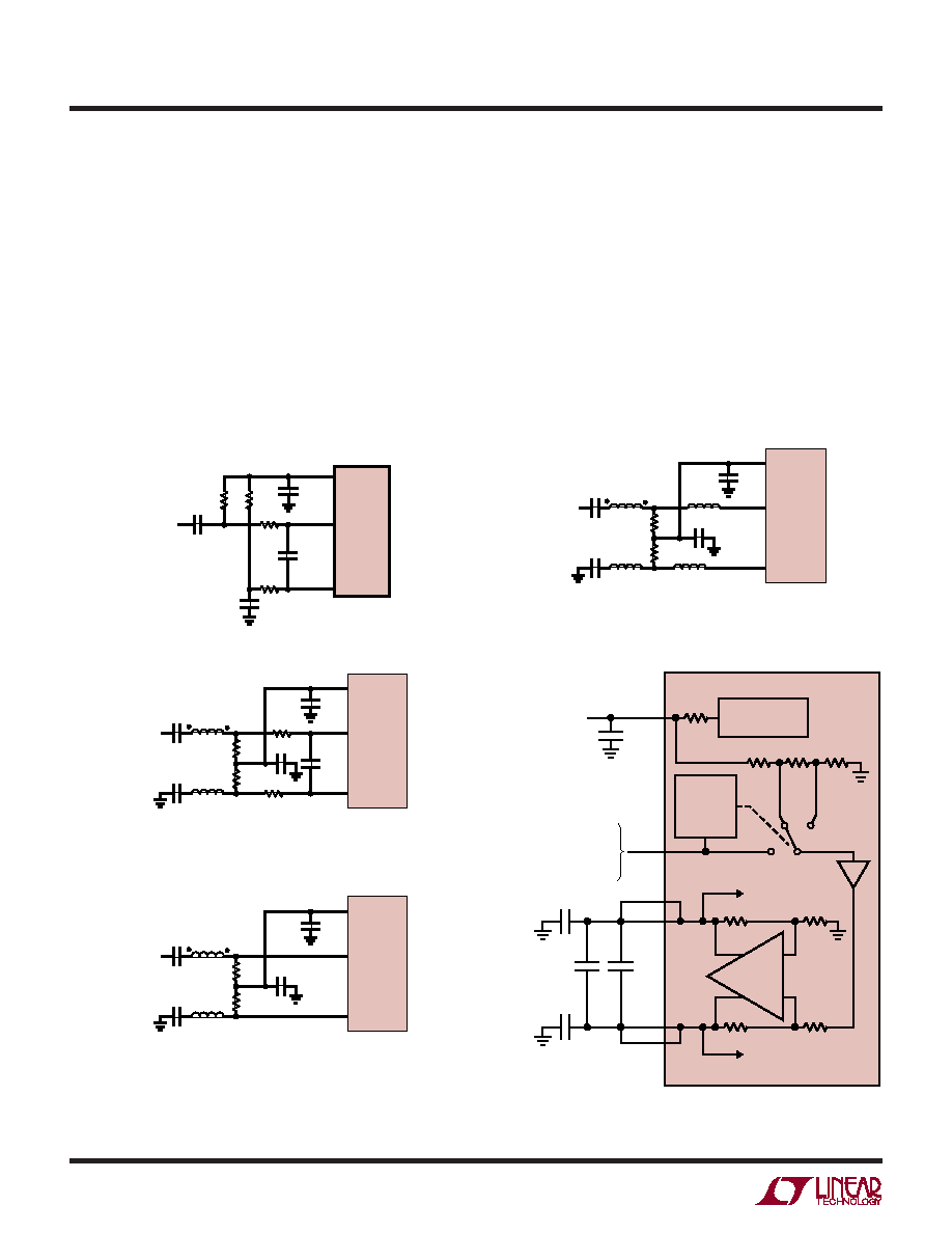
Reference Operation
Figure 9 shows the LTC2239 reference circuitry consisting
of a 1.5V bandgap reference, a difference amplifier and
switching and control circuit. The internal voltage refer-
ence can be configured for two pin selectable input ranges
of 2V (
±1Vdifferential)or1V(±0.5Vdifferential).Tyingthe
SENSE pin to VDD selects the 2V range; tying the SENSE
pin to VCM selects the 1V range.
Figure 5. Single-Ended Drive
25
0.1
F
ANALOG
INPUT
VCM
AIN
+
AIN
–
1k
12pF
2239 F05
2.2
F
1k
25
0.1
F
LTC2239
Figure 5 shows a single-ended input circuit. The imped-
ance seen by the analog inputs should be matched. This
circuit is not recommended if low distortion is required.
The 25
resistorsand12pFcapacitorontheanaloginputs
serve two purposes: isolating the drive circuitry from the
sample-and-hold charging glitches and limiting the
wideband noise at the converter input.
For input frequencies above 70MHz, the input circuits of
Figure 6, 7 and 8 are recommended. The balun trans-
former gives better high frequency response than a flux
coupled center tapped transformer. The coupling capaci-
tors allow the analog inputs to be DC biased at 1.5V. In
Figure 6. Recommended Front End Circuit for
Input Frequencies Between 70MHz and 170MHz
25
25
12
12
0.1
F
AIN
+
AIN
–
8pF
2.2
F
VCM
LTC2239
ANALOG
INPUT
0.1
F
0.1
F
T1
T1 = MA/COM, ETC 1-1-13
RESISTORS, CAPACITORS
ARE 0402 PACKAGE SIZE
2239 F06
25
25
0.1
F
AIN
+
AIN
–
2.2
F
VCM
LTC2239
ANALOG
INPUT
0.1
F
0.1
F
T1
T1 = MA/COM, ETC 1-1-13
RESISTORS, CAPACITORS
ARE 0402 PACKAGE SIZE
2239 F07
25
25
0.1
F
AIN
+
AIN
–
2.2
F
VCM
LTC2239
ANALOG
INPUT
0.1
F
0.1
F
T1
T1 = MA/COM, ETC 1-1-13
RESISTORS, CAPACITORS, INDUCTORS
ARE 0402 PACKAGE SIZE
2239 F08
6.8nH
Figure 7. Recommended Front End Circuit for
Input Frequencies Between 170MHz and 300MHz
VCM
REFH
SENSE
TIE TO VDD FOR 2V RANGE;
TIE TO VCM FOR 1V RANGE;
RANGE = 2 VSENSE FOR
0.5V < VSENSE < 1V
1.5V
REFL
2.2
F
2.2
F
INTERNAL ADC
HIGH REFERENCE
BUFFER
0.1
F
2239 F09
LTC2239
4
DIFF AMP
1
F
1
F
INTERNAL ADC
LOW REFERENCE
1.5V BANDGAP
REFERENCE
1V
0.5V
RANGE
DETECT
AND
CONTROL
Figure 9. Equivalent Reference Circuit
Figure 8. Recommended Front End Circuit for
Input Frequencies Above 300MHz
发布紧急采购,3分钟左右您将得到回复。
相关PDF资料
LTC2240CUP-12#PBF
IC ADC 12BIT 170MSPS 64-QFN
LTC2240IUP-10#PBF
IC ADC 10BIT 170MSPS 64-QFN
LTC2241IUP-10#PBF
IC ADC 10BIT 210MSPS 64-QFN
LTC2242IUP-10#PBF
IC ADC 10BIT 250MSPS 64-QFN
LTC2245IUH#TRPBF
IC ADC 14BIT 10MSPS 3V 32-QFN
LTC2249IUH#TRPBF
IC ADC 14BIT 80MSPS LP 32-QFN
LTC2251IUH#PBF
IC ADC 10-BIT 125MSPS 3V 32-QFN
LTC2253IUH#TRPBF
IC ADC 12BIT 125MSPS 3V 32-QFN
相关代理商/技术参数
LTC2239CUH#TRPBF
功能描述:IC ADC 10BIT 80MSPS 3V 32-QFN RoHS:是 类别:集成电路 (IC) >> 数据采集 - 模数转换器 系列:- 标准包装:1,000 系列:- 位数:16 采样率(每秒):45k 数据接口:串行 转换器数目:2 功率耗散(最大):315mW 电压电源:模拟和数字 工作温度:0°C ~ 70°C 安装类型:表面贴装 封装/外壳:28-SOIC(0.295",7.50mm 宽) 供应商设备封装:28-SOIC W 包装:带卷 (TR) 输入数目和类型:2 个单端,单极
LTC2239IUH
制造商:LINER 制造商全称:Linear Technology 功能描述:10-Bit, 80Msps Low Noise 3V ADC
LTC2239IUH#PBF
功能描述:IC ADC 10-BIT 80MSPS 3V 32-QFN RoHS:是 类别:集成电路 (IC) >> 数据采集 - 模数转换器 系列:- 标准包装:1,000 系列:- 位数:12 采样率(每秒):300k 数据接口:并联 转换器数目:1 功率耗散(最大):75mW 电压电源:单电源 工作温度:0°C ~ 70°C 安装类型:表面贴装 封装/外壳:24-SOIC(0.295",7.50mm 宽) 供应商设备封装:24-SOIC 包装:带卷 (TR) 输入数目和类型:1 个单端,单极;1 个单端,双极
LTC2239IUH#TRPBF
功能描述:IC ADC 10BIT 80MSPS 3V 32-QFN RoHS:是 类别:集成电路 (IC) >> 数据采集 - 模数转换器 系列:- 标准包装:1,000 系列:- 位数:12 采样率(每秒):300k 数据接口:并联 转换器数目:1 功率耗散(最大):75mW 电压电源:单电源 工作温度:0°C ~ 70°C 安装类型:表面贴装 封装/外壳:24-SOIC(0.295",7.50mm 宽) 供应商设备封装:24-SOIC 包装:带卷 (TR) 输入数目和类型:1 个单端,单极;1 个单端,双极
LTC2240-10
制造商:LINER 制造商全称:Linear Technology 功能描述:14-Bit 250Msps/ 210Msps/170Msps ADCs
LTC2240-12
制造商:LINER 制造商全称:Linear Technology 功能描述:14-Bit 250Msps/ 210Msps/170Msps ADCs
LTC2240CUP-10
制造商:LINER 制造商全称:Linear Technology 功能描述:10-Bit, 170Msps ADC
LTC2240CUP-10#PBF
功能描述:IC ADC 10BIT 170MSPS 64-QFN RoHS:是 类别:集成电路 (IC) >> 数据采集 - 模数转换器 系列:- 标准包装:1 系列:- 位数:14 采样率(每秒):83k 数据接口:串行,并联 转换器数目:1 功率耗散(最大):95mW 电压电源:双 ± 工作温度:0°C ~ 70°C 安装类型:通孔 封装/外壳:28-DIP(0.600",15.24mm) 供应商设备封装:28-PDIP 包装:管件 输入数目和类型:1 个单端,双极